- 您现在的位置:买卖IC网 > Sheet目录1212 > DS1864K (Maxim Integrated Products)KIT EVAL FOR DS1864
�� �
�
�SFP� Laser� Controller� and�
�Diagnostic� IC�
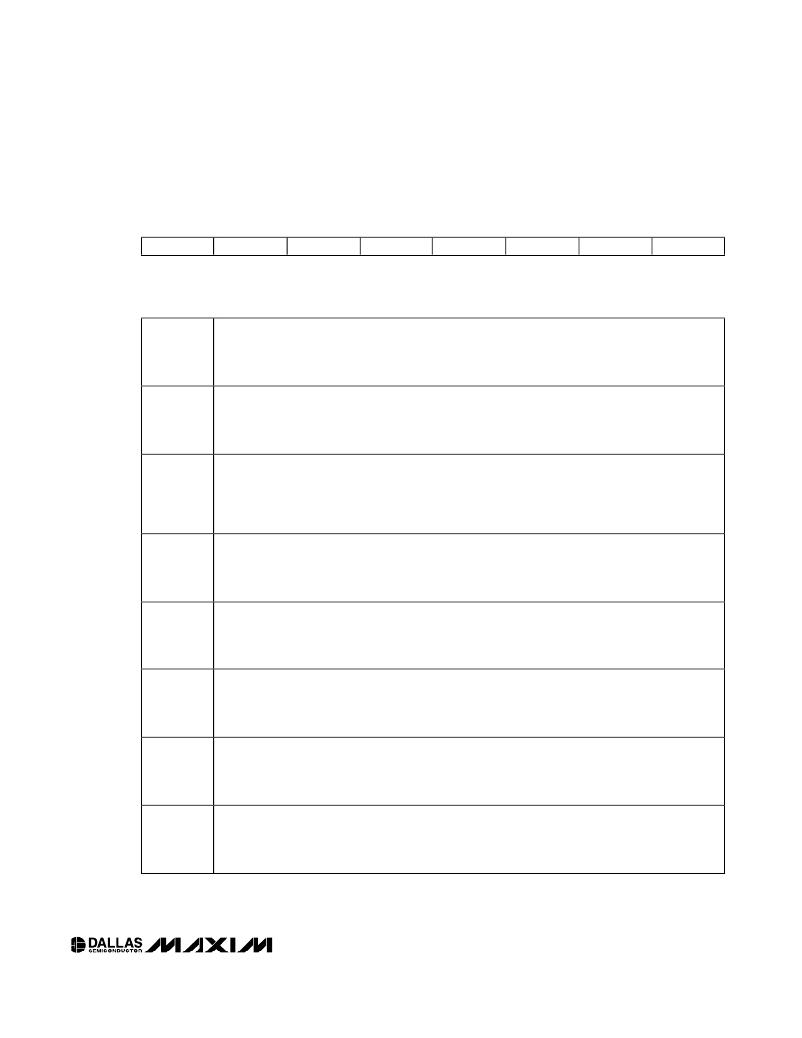
�Table� 05h,� D1h:� PW1� Password� Write-Enable� Byte�
�FACTORY� DEFAULT:�
�MEMORY� TYPE:�
�00h�
�Shadowed� Memory� (SEE)�
�2�
�D1h�
�7�
�2� 6�
�2� 5�
�2� 4�
�2� 3�
�2� 2�
�2� 1�
�2� 0�
�bit7�
�bit0�
�This� byte� configures� the� Write� protection� of� PW1.� This� is� discussed� in� more� detail� in� the� Memory� Protection� and� Password� s� ection.�
�When� this� bit� is� set,� PW1� Write� protection� is� enabled� for� the� memory� block� consisting� of� registers� D0h�
�bit7�
�bit6�
�bit5�
�bit4�
�bit3�
�bit2�
�bit1�
�bit0�
�through� D6h� in� the� Main� Device� memory,� Table� 05h.�
�0� =� Memory� is� unprotected� (PW1� level).�
�1� =� Memory� is� protected� (PW1� level).�
�When� this� bit� is� set,� PW1� Write� protection� is� enabled� for� the� memory� block� consisting� of� registers� F8h�
�through� FFh� in� the� Main� Device� memory,� Table� 05h.�
�0� =� Memory� is� unprotected� (PW1� level).�
�1� =� Memory� is� protected� (PW1� level).�
�When� this� bit� is� set,� PW1� Write� protection� is� enabled� for� the� memory� block� consisting� of� registers� 80h�
�through� C7h� in� the� Main� Device� memory,� Table� 04h� (Table� 01h� in� DS1859� configuration),� Table� 02h,�
�and� Table� 03h.�
�0� =� Memory� is� unprotected� (PW1� level).�
�1� =� Memory� is� protected� (PW1� level).�
�When� this� bit� is� set,� PW1� Write� protection� is� enabled� for� the� memory� block� consisting� of� registers� F8h�
�through� FFh� in� the� Main� Device� memory,� Table� 01h� (Table� 00h� in� DS1859� configuration).�
�0� =� Memory� is� unprotected� (PW1� level).�
�1� =� Memory� is� protected� (PW1� level).�
�When� this� bit� is� set,� PW1� Write� protection� is� enabled� for� the� memory� block� consisting� of� registers� 80h�
�through� F7h� in� the� Main� Device� memory,� Table� 01h� (Table� 00h� in� DS1859� configuration).�
�0� =� Memory� is� unprotected� (PW1� level).�
�1� =� Memory� is� protected� (PW1� level).�
�When� this� bit� is� set,� PW1� Write� protection� is� enabled� for� the� memory� block� consisting� of� registers� 00h�
�through� 7Ah� in� the� Main� Device� memory.�
�0� =� Memory� is� unprotected� (PW1� level).�
�1� =� Memory� is� protected� (PW1� level).�
�When� this� bit� is� set,� PW1� Write� protection� is� enabled� for� the� memory� block� consisting� of� registers� 80h�
�through� FFh� in� the� Auxiliary� Device� memory� on� I� 2� C� slave� address� A0h.�
�0� =� Memory� is� unprotected� (PW1� level).�
�1� =� Memory� is� protected� (PW1� level).�
�When� this� bit� is� set,� PW1� Write� protection� is� enabled� for� the� memory� block� consisting� of� registers� 00h�
�through� 7Fh� in� the� Auxiliary� Device� memory� of� I� 2� C� slave� ddress� A0h.�
�0� =� Memory� is� unprotected� (PW1� level).�
�1� =� Memory� is� protected� (PW1� level).�
�____________________________________________________________________�
�61�
�发布紧急采购,3分钟左右您将得到回复。
相关PDF资料
DS21349DK
KIT DESIGN FOR DS21349
DS21352DK
KIT DESIGN FOR DS21352
DS21354DK
KIT DESIGN FOR DS21354
DS21458DK
KIT DESIGN FOR G511DS21458
DS2156DK
KIT DESIGN FOR DS2156
DS21Q348DK
KIT DESIGN FOR DS21Q348
DS21Q55DK
KIT DESIGN FOR DS21Q55
DS2436K
KIT DEMO BATT ID/MON CHIP DS2436
相关代理商/技术参数
DS1864T
制造商:Maxim Integrated Products 功能描述:DUAL TMP CTRL DAC+MONITORS,QFN - Rail/Tube
DS1864T+
功能描述:激光驱动器 SFP Laser Controller & Diagnostic IC RoHS:否 制造商:Micrel 数据速率:4.25 Gbps 工作电源电压:3 V to 3.6 V 电源电流:80 mA 最大工作温度:+ 85 C 封装 / 箱体:QFN-16 封装:Tube
DS1864T+T&R
制造商:Maxim Integrated Products 功能描述:DUAL TMP CTRL DAC+MON QFN T&R LF - Tape and Reel 制造商:Maxim Integrated Products 功能描述:IC LASER CTRLR 1CHAN 5.5V 28TQFN
DS1864T+T&R
功能描述:激光驱动器 SFP Laser Controller & Diagnostic IC RoHS:否 制造商:Micrel 数据速率:4.25 Gbps 工作电源电压:3 V to 3.6 V 电源电流:80 mA 最大工作温度:+ 85 C 封装 / 箱体:QFN-16 封装:Tube
DS1865
制造商:MAXIM 制造商全称:Maxim Integrated Products 功能描述:PON Triplexer Control and Monitoring Circuit
DS1865_09
制造商:MAXIM 制造商全称:Maxim Integrated Products 功能描述:PON Triplexer Control and Monitoring Circuit
DS1865E+
制造商:Maxim Integrated Products 功能描述:- Rail/Tube
DS1865E+T&R
制造商:Maxim Integrated Products 功能描述:- Tape and Reel